
- English
- Español
- Português
- русский
- Français
- 日本語
- Deutsch
- tiếng Việt
- Italiano
- Nederlands
- ภาษาไทย
- Polski
- 한국어
- Svenska
- magyar
- Malay
- বাংলা ভাষার
- Dansk
- Suomi
- हिन्दी
- Pilipino
- Türkçe
- Gaeilge
- العربية
- Indonesia
- Norsk
- تمل
- český
- ελληνικά
- український
- Javanese
- فارسی
- தமிழ்
- తెలుగు
- नेपाली
- Burmese
- български
- ລາວ
- Latine
- Қазақша
- Euskal
- Azərbaycan
- Slovenský jazyk
- Македонски
- Lietuvos
- Eesti Keel
- Română
- Slovenski
- मराठी
- Srpski језик
중국 CVD SIC 제조업체, 공급업체, 공장
CVD SiC is a vacuum deposition process used to produce high-purity solid materials. This process is often used in semiconductor manufacturing to form thin films on wafer surfaces. During the chemical vapor deposition (CVD) process for producing silicon carbide (SiC), a substrate is exposed to one or more volatile precursors, which chemically react on the substrate surface to form the desired SiC deposit. Among the various methods for producing SiC, CVD produces products with high uniformity and purity, and offers strong process controllability.
Simply put, CVD SiC refers to SiC produced via the chemical vapor deposition (CVD) process. In this process, gaseous precursors, typically containing silicon and carbon, react in a high-temperature reactor to deposit a thin SiC film onto a substrate. CVD SiC is valued for its exceptional properties, including high thermal conductivity, chemical inertness, mechanical strength, and resistance to thermal shock and wear. These properties make chemical vapor deposited (CVD) silicon carbide (SiC) ideal for demanding applications such as semiconductor manufacturing, aerospace components, armor, and high-performance coatings. This material's exceptional durability and stability under extreme conditions ensure its effectiveness in improving the performance and lifespan of advanced technologies and industrial systems.
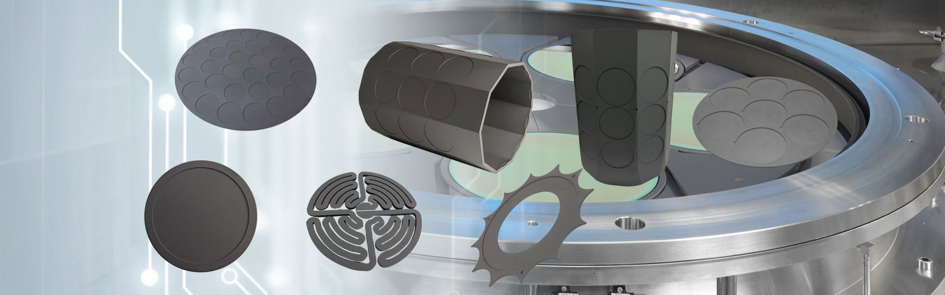
CVD SiC materials, due to their unique combination of excellent thermal, electrical, and chemical properties, are well-suited for applications in the semiconductor industry, where high-performance materials are required. Chemical vapor deposited (CVD) silicon carbide (SiC) components are widely used in etching equipment, MOCVD equipment, Si and SiC epitaxy equipment, and rapid thermal processing equipment.
The largest market segment for CVD SiC components is etching equipment components. Due to its low reactivity to chlorine- and fluorine-containing etching gases and its electrical conductivity, CVD silicon carbide (SiC) is an ideal material for components such as focus rings in plasma etching equipment. CVD silicon carbide (SiC) components in etching equipment include focus rings, gas showerheads, trays, edge rings.
Take the focus ring, for example. This critical component is placed outside the wafer and in direct contact with it. Voltage is applied to the ring to focus the plasma passing through it, thereby focusing the plasma on the wafer and improving processing uniformity. Traditionally, focus rings are made of silicon or quartz. However, with the advancement of integrated circuit miniaturization, the demand for and importance of etching processes in integrated circuit manufacturing continues to increase. The power and energy of the plasma used for etching are also increasing, especially in capacitively coupled plasma (CCP) etching equipment, which requires even higher plasma energies. Consequently, focus rings made of silicon carbide are becoming increasingly popular.
Due to the high performance of CVD SiC and its ability to be sliced into very thin sections, it can also benefit sputter targets and all types of electrodes.
Process of Chemical Vapor Deposition (CVD)
CVD is a process that transforms a material from a gas phase to a solid phase, used to form a thin film or coating on a substrate surface. The following are the basic steps in CVD:
1. Substrate Preparation
Choose an appropriate substrate material and perform the appropriate cleaning and surface treating to produce a clean, flat surface with good adhesion.
2. Reactive Gas Preparation
Prepare the necessary amount of reactive gas or vapor and inject it into the deposition chamber by some means (gas supply system). The reactive gas can be an organic compound, a metal-organic precursor, inert gas, or other gaseous species.
3. Deposition Reaction
If all instrumentation is setup correctly the CVD process will begin under the pre-defined reaction conditions. The reactive gas that has been injected into the chamber will undergo some chemical or physical reaction on the substrate surface to form a deposit onto the substrate surface. The deposit formation can be the result of several types of processes depending on the deposition method, these include vapor-phase thermal decomposition, chemical reaction, sputtering, epitaxial growth, etc.
4. Control and Monitoring
At the same time during the deposition process, certain deposition parameters need to be controlled and monitored in real time if the observer wishes to ensure the best possible properties in the film are maintained. These include relevant temperature measurement, pressure monitoring, and regulation of gas flow, all the while aiming to keep the desired reaction conditions stable and constant.
5. Deposition Completion and Post-Processing
When either the deposition time, predetermined thickness, or method selected, is achieved the introduction of the reaction gas can be ceased and deposition process ended. Following the deposition, several pertinent post-processing methods (annealing, structural modifications, surface treatment, etc.) should be performed to improve the film performance/quality.
It's important to note that the specific vapor deposition process can vary depending on the deposition technology, material type, and application requirements. However, the basic process outlined above covers most common vapor deposition steps.


- View as

상부 전극 접지 링
Semicorex 상부 전극 접지 링은 고급 반도체 에칭 및 증착 시스템에서 전위를 안정화하고 균일한 플라즈마 분포를 지원하는 초고순도 CVD SiC 플라즈마 제어 부품입니다. Semicorex는 전 세계적으로 정밀 CVD SiC 접지 링과 플라즈마 직면 반도체 부품을 공급하여 선도적인 반도체 장비 제조업체를 위한 맞춤형 치수, 전기적 특성 및 안정적인 글로벌 배송을 제공합니다.*
더 읽어보기문의 보내기


반도체용 세라믹 포커스 링
반도체용 Semicorex 세라믹 포커스 링은 고강도 플라즈마 에칭 환경을 위해 특별히 설계된 CVD SiC 재료로 만든 고성능 링 부품입니다. Semicorex는 업계 최고의 반도체용 CVD SiC 세라믹 포커스 링 제조업체입니다. 귀하의 문의를 기다리겠습니다.
더 읽어보기문의 보내기
2L10-506419-21용 CVD SiC 포커스 링
고성능 CVD SiC 재료로 제작된 2L10-506419-21용 Semicorex CVD SiC 포커스 링은 정밀 반도체 에칭 공정에 사용되는 TEL VIGUS RK4 장비용으로 특별히 설계된 중요한 링 부품입니다. Semicorex를 선택하면 정확하고 균일한 에칭 결과를 달성하기 위한 이상적인 CVD SiC 솔루션을 얻을 수 있습니다.
더 읽어보기문의 보내기
고체 실리콘 카바이드 핀
Semicorex 솔리드 탄화규소 핀은 주로 반도체 열처리 장비의 고온로에 사용되는 솔리드 CVD SiC를 정밀 가공한 고성능 부품입니다. Semicorex는 소중한 고객에게 시장 최고의 품질을 갖춘 맞춤형 엔지니어링 탄화규소 핀을 제공하기 위해 최선을 다하고 있으며 중국에서 장기적인 파트너가 되기를 기대합니다.
더 읽어보기문의 보내기
Semicorex는 수년 동안 CVD SIC을(를) 생산해 왔으며 중국의 전문 CVD SIC 제조업체 및 공급업체 중 하나입니다. 대량 포장을 제공하는 당사의 고급 내구성 제품을 구매하면 대량의 빠른 배송을 보장합니다. 수년에 걸쳐 우리는 고객에게 맞춤형 서비스를 제공했습니다. 고객은 우리 제품과 우수한 서비스에 만족합니다. 우리는 진심으로 귀하의 신뢰할 수 있는 장기 비즈니스 파트너가 되기를 기대합니다! 우리 공장에서 제품을 구입하는 것을 환영합니다.